nano-world)의 정복을 가능케 하였으며, 나노입자(nano-particle), 나노코팅(nano-coating), 나노섬유(nano-fiber)의 활용을 통한 혜택은 현재 많은 이들에 의해 입증되고 있는 중이다.
나노 기술을 이용한 의류 가공에 있어서, 후 가공 공정 중 나노구조를 발현시키는 방법이 있다. 나노물질이나 나노입자를 가공제
nanotechnology, especially nanoparticles that can carry the drug molecules to the target safely.
5.2.2 Nanocarriers - Nanoparticles
Before starting with the functionalization of nanoparticles, it is important to keep in mind a range of useful properties we wish to have in any drug delivery across the BBB(Blood brain barrier). In this context, owing to their small size, customizable surfac
Nanoparticles present possible dangers
- due to the high surface to volume ratio
pass through cell membranes in organisms
Smaller nanoparticles evinced increased cytotoxicity.
Self-assembly :
process that disordered system of components forms an organized structure or pattern
The device is switched on - >
the pump pushes ions across the lipid membrane,
Nano Imprint Lithography)는 열 또는 UV를 소스(source)로하여 레지스트(resist)의 유동성을 이용해서 나노 사이즈의 패턴을 전사하는 방법으로 기존의 Deep UV, EUV, X-ray를 사용한 방법보다 비용이 저렴하며 대량 생산이 가능하다는 장점이 있다.
2. 본론
⑴ Nano Imprint Lithography (NIL) 의 기본 원리
나노 임
S.W.O.T.
.
.
.바이오센서에 나노기술을 접목시킨 초고감도 센서▶ 전 세계적 태동기기술
원천기술 확보와 특허분쟁도 피할 수 있을 거라 기대됨
원천기술 확보로 40억 달러의 바이오센서 시장에 진입하면 엄청난 부가가치 창출
나노 기술을 이용하여 기존 바이오센서의 한계 극복 및 성능 개선
Sol-Gel법
Sol: 액상에 고체입자가 분산되어 있는 콜로이드
- Aerosol : 기상에 고체입자 혹은 액적이 분산
- Emulsion : 액상에 액적이 분산
Gel: Sol의 입자들이 물리적인 힘으로 연결되어
형성(gelation)된 망상조직.
- Xerogel : 상압에서 Sol용액을 증발시켜 얻은 젤
- Aerogel : 고온 감압 하에서
remove large debris such as sticks, leaves, trash and other large particles
water stored in reservoirs for periods between a few days and many months to allow natural biological purification to take place
salts are treated with soda-ash (Na2CO3) to precipitate CaCO3 out utilizing the common-ion effect
chlorinated to minimize the growth of fouling organisms on the pipe-work and tanks
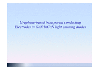
We investigated graphene-based transparent electrodes for InGaN/GaN light emitting diodes(LED). Nano-dotted layer of Ag and Ni were inserted between p-GaN and graphene to achieve low contact resistance and high transmittance. Heat treated Ag layer/graphene had low contact resistance of 0.7~1.2Ω/cm2, and we could achieve better luminance for GaN-based LED. However, for patterned Ni layer/graphene
*’Nano’ means….
Nanometer: one billionth of a meter
Nano-: prefix comes from the Greek word for ‘dwarf’
Chemical, physical, and biological properties that differ from those of their larger, or bulk counterparts
Nanotechnology: The National Nanotechnology Initiative(NNI)-> the science of materials and phenomena in the range of 1 to 100nm in diameter
*Features of ‘nanoparticles